Key Patents
-
Via-post
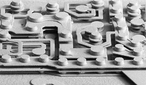
 Electroplated copper pillar replaces traditional machine drill and laser drill as the interconnection mode between layers of substrate.
Electroplated copper pillar or copper block as the vertical channel for heat dissipation of chip.
Electroplated copper pillar or copper block as the fabrication method of cavity
Electroplated copper pillar or bump as the connector of chip and substrate.
Electroplated copper pillar replaces traditional machine drill and laser drill as the interconnection mode between layers of substrate.
Electroplated copper pillar or copper block as the vertical channel for heat dissipation of chip.
Electroplated copper pillar or copper block as the fabrication method of cavity
Electroplated copper pillar or bump as the connector of chip and substrate.
-
Coreless packaging substrate
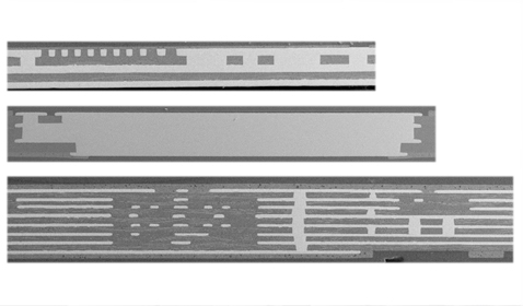 No need to use traditional core material
Build up process starting from any layer
Interconnection between any layers based on copper pillar method
Interconnect by arbitrary Shape of solid copper based on copper pillar method.
Packaging substrate technology for ultra-thin dielectric layer stacking.
No need to use traditional core material
Build up process starting from any layer
Interconnection between any layers based on copper pillar method
Interconnect by arbitrary Shape of solid copper based on copper pillar method.
Packaging substrate technology for ultra-thin dielectric layer stacking.
-
Embedded packaging of active and passive
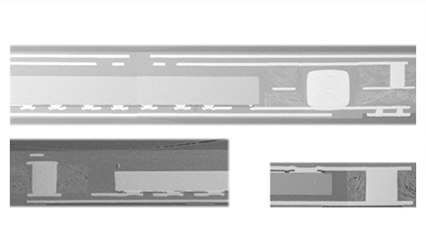 Reduce the three-dimensional scale of the package.
Embedded active and passive components in substrate at the same time, forming system in package
Use copper pillar technology to conduct chip I/O and all layers of circuits, with high reliability
Reduce the three-dimensional scale of the package.
Embedded active and passive components in substrate at the same time, forming system in package
Use copper pillar technology to conduct chip I/O and all layers of circuits, with high reliability